FT7001 USB DIO Card
l 96 Bidirection DIO
l Compatible TTL and CMOS input levels
l Digital output up to ±24mA
l Grouping Strategy: 8bits X 12 groups
l Providing two 5VDC * Max 1A power output
ABSTRACT:
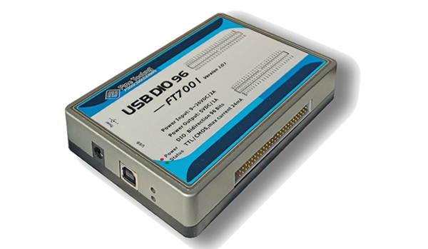
FT7001 is designed for industrial projects that require a large amount of IO signals. FT7001 adopts USB 2.0 high-speed communication. Plug and play installation reduces the setup and configuration time to the greatest extent, which not only ensures convenient installation for users, but also meets the real-time requirements of data transmission as far as possible. The standard configuration has a 12VDC power adapter and a USB2.0 high-speed transmission Type A to B cable (MPN: FTUABMM15001).
The product supports up to 96 bidirectional IO channels, compatible TTL and CMOS input levels, and digital output up to ±24mA.
Free support for FT Studio and HWSuit tools.
System support: Windows XP/10 Linux
Software compatibility: LabVIEW Visual Studio FTStudio
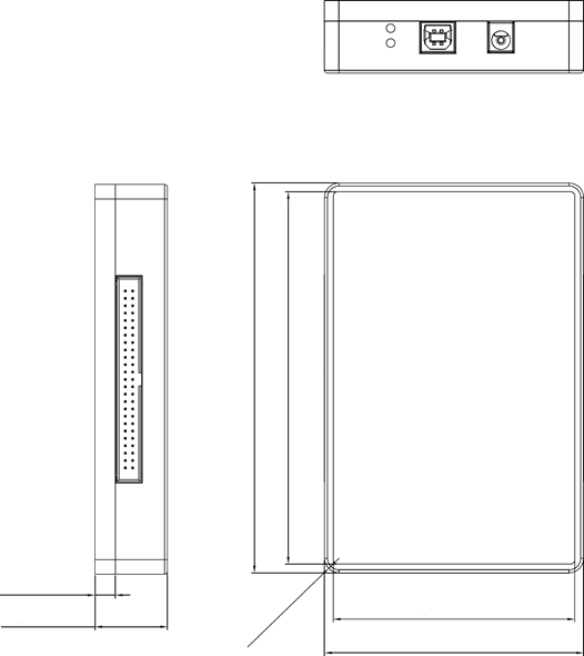
n OUTLINE DIMENSION:

Picture 1 USB DIO FT7001 DIMENSION
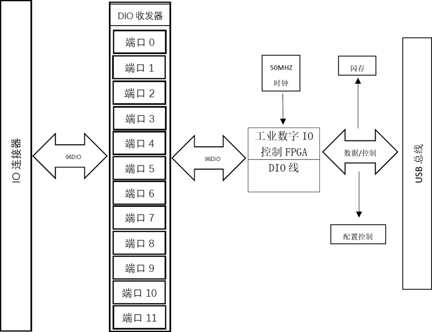
n INTERFACE DEFINITION:

Picture 2 USB DIO FT7001 IO Interface Structure
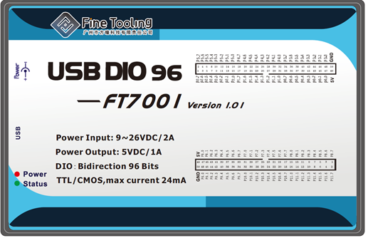
The IO interface of the product uses two IDC 50 2.54mm sockets. Details on the signals available for the connector can also be seen in the product housing label.
Table 1 Connector Pins Definition
CON1 – 50Pin |
| CON2 – 50Pin |
P2.7 | 1 | 2 | P5.7 | P8.7 | 1 | 2 | P11.7 |
P2.6 | 3 | 4 | P5.6 | P8.6 | 3 | 4 | P11.6 |
P2.5 | 5 | 6 | P5.5 | P8.5 | 5 | 6 | P11.5 |
P2.4 | 7 | 8 | P5.4 | P8.4 | 7 | 8 | P11.4 |
P2.3 | 9 | 10 | P5.3 | P8.3 | 9 | 10 | P11.3 |
P2.2 | 11 | 12 | P5.2 | P8.2 | 11 | 12 | P11.2 |
P2.1 | 13 | 14 | P5.1 | P8.1 | 13 | 14 | P11.1 |
P2.0 | 15 | 16 | P5.0 | P8.0 | 15 | 16 | P11.0 |
P1.7 | 17 | 18 | P4.7 | P7.7 | 17 | 18 | P10.7 |
P1.6 | 19 | 20 | P4.6 | P7.6 | 19 | 20 | P10.6 |
P1.5 | 21 | 22 | P4.5 | P7.5 | 21 | 22 | P10.5 |
P1.4 | 23 | 24 | P4.4 | P7.4 | 23 | 24 | P10.4 |
P1.3 | 25 | 26 | P4.3 | P7.3 | 25 | 26 | P10.3 |
P1.2 | 27 | 28 | P4.2 | P7.2 | 27 | 28 | P10.2 |
P1.1 | 29 | 30 | P4.1 | P7.1 | 29 | 30 | P10.1 |
P1.0 | 31 | 32 | P4.0 | P7.0 | 31 | 32 | P10.0 |
P0.7 | 33 | 34 | P3.7 | P6.7 | 33 | 34 | P9.7 |
P0.6 | 35 | 36 | P3.6 | P6.6 | 35 | 36 | P9.6 |
P0.5 | 37 | 38 | P3.5 | P6.5 | 37 | 38 | P9.5 |
P0.4 | 39 | 40 | P3.4 | P6.4 | 39 | 40 | P9.4 |
P0.3 | 41 | 42 | P3.3 | P6.3 | 41 | 42 | P9.3 |
P0.2 | 43 | 44 | P3.2 | P6.2 | 43 | 44 | P9.2 |
P0.1 | 45 | 46 | P3.1 | P6.1 | 45 | 46 | P9.1 |
P0.0 | 47 | 48 | P3.0 | P6.0 | 47 | 48 | P9.0 |
+5V | 49 | 50 | GND | +5V | 49 | 50 | GND |

Picture 3 USB DIO FT7001 Product Housing Label
n ELECTRICAL CHARACTERISTICS:
FT7001 can be set as an input or output by ports. Users configure it directly through the API interface of FT7001. After startup and initialization, all IOs are in input weak pull-up state.
Table 2 Absolute Maximum Ratings
Parameters | MIN | MAX | UNIT |
VI (Input voltage range) | -0.5 | 5.5 | V |
IIC (Input clamp current) |
| -50 | mA |
Vo (Input voltage range) | -0.5 | 5.5 | V |
IOC (Output clamp current) |
| ±50 | mA |
Tips: Stresses beyond those listed under Absolute Maximum Ratings may cause permanent damage to the device. These are stress ratings only, and functional operation of the device at these or any other conditions beyond those indicated under Recommended Operating Conditions is not implied. Exposure to absolute-maximum-rated conditions for extended periods may affect device reliability.
Table 3 Recommended Operating Conditions
Parameters | MIN | MAX | UNIT |
VI (Input voltage range) | -0.5 | 5.5 | V |
IIC (Input clamp current) |
| -24 | mA |
Vo (Input voltage range) | -0.5 | 5.5 | V |
IOC (Output clamp current) |
| ±24 | mA |
For details information, please CLICK HERE TO DOWNLOAD FT7001 User manual.
For more information please contact: 020-82108945-8002
